


HBM Memory

TSV Technology Iteration in HBM – New Requirements for Equipment Suppliers

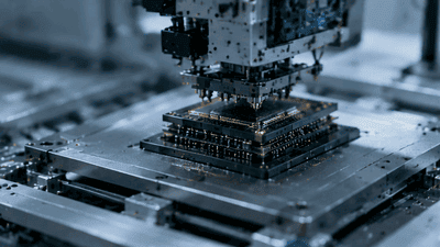
Through successive HBM generations the through-silicon via (TSV) has evolved from a tactical enabling feature into a strategic differentiator. As HBM moves from HBM2E and HBM3 to HBM3e and HBM4, TSVs must support finer pitches, lower parasitics, higher thermal conduction needs, and coexistence with hybrid-bond planes. These requirements cascade into new expectations for equipment suppliers across lithography, etch, deposition, CMP, inspection, and metrology.

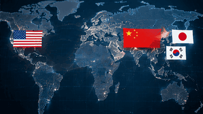
Global HBM Patent Landscape Competition: The US-China-Japan-Korea Power Game

High-Bandwidth Memory (HBM) has become one of the most strategically important technologies in the AI and high‑performance computing era. Patents around HBM architectures, hybrid bonding, TSVs, interposers, thermal solutions and test methods now form a dense web of intellectual property that shapes who can manufacture, license and profit from AI memory at scale. The global HBM patent landscape is increasingly a power game among the United States, China and Japan, layered on top of Korean and Taiwanese industrial strengths.

Breakthroughs in Wafer Warpage Control During HBM Manufacturing

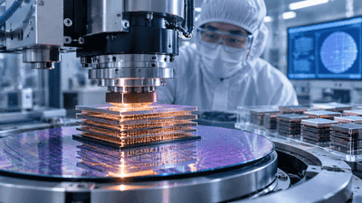
Wafer warpage has long been a critical yield and reliability concern in advanced semiconductor packaging, and it is especially consequential for High Bandwidth Memory (HBM). HBM’s stacked-die architecture, use of through-silicon vias (TSVs), and reliance on precise bonding and micro-bump formation all amplify the impact of any deviation from flatness. Recent breakthroughs in warpage control—spanning materials science, process engineering, metrology, and modeling—are improving yields, reducing costs, and enabling larger HBM stacks with higher interconnect densities.

Big 3 Memory Makers’ HBM CapEx Share Exceeds 50% for the First Time in 2026

In 2026 the semiconductor landscape reached a decisive inflection: the combined capital expenditure (capex) directed by the industry’s Big Three memory makers—SK Hynix, Samsung, and Micron—toward High-Bandwidth Memory (HBM) and its enabling packaging technologies exceeded 50% of total industry HBM-capex for the first time. This milestone matters because it signals concentrated investment toward premium memory and packaging ecosystems that underpin AI accelerators, HPC clusters, and advanced datacenter architectures.

  • 1
  • 2
  • 3